BIC test
This section contains the nanofabrication steps I followed to test the nanofabrication recipes for the realization of a photonic pattern hosting BICs composed of nanometric circular holes.
Wafer: 300 nm SiN, low-stress Resist: CSAR
Past tests overview
During my master's thesis I realized the same pattern on a 300 nm high-stress SiN wafer exposed with a 150 \(\mu\)C/cm\(^2\) dose and after a SEM analysis we realized that the holes were overexposed and had an irregular shape, so we decided to lower the dose and change the filling mode from inward to outward.
Then, during some preliminary tests realized using an adhesivant+CSAR resist layer I got cracks around square markers after EBL exposure, so I decided to remove the adhesivant layer for the following tests.
Furthermore, I had problems with the EBL machine giving memory errors due to heavy CAD files, so I decided to reduce the tolerance parameter from 0.001 to 0.01 characterizing the holes precision with the ellipse function of the gdstk package and reduced the number of holes per pattern.
STEP 1
18/05/2026 Spin coating, EBL exposure, Development
| Spin&bake | |
|---|---|
| AR.P 6200.13 | 2000 RPM, 1'; 150°C, 1' |
| EBL |
|---|
| EHT: 30 kV |
| aperture: 30 \(\mu\)m |
| Dose: 140 \(\mu\)C/cm\(^2\) |
| step-size: 20 nm |
| filling mode: concentric, outward |
ERROR: exposure stopped before ending
| Develop | |
|---|---|
| AR 600-546 | 1' 30'', stop in IPA |
20/05/2026 RIE etching
| RIE |
|---|
| \(SF_6\)/\(O_2\): 32/8 sccm |
| 50 W, time: 4' |
21/05/2026 SEM imaging
The holes have been etched to a depth of 250 nm so they weren't opened yet. We decided to repeat the test and try with longer etching times.
STEP 2
25/05/2026 Spin coating, EBL exposure, Development
| Spin&bake | |
|---|---|
| AR.P 6200.13 | 2000 RPM, 1'; 150°C, 1' |
To avoid the error I got last time during EBL I changed the CAD file and decided to draw circles as 64vertex-polygons and the exposure didn't stop this time.
| EBL |
|---|
| EHT: 30 kV |
| aperture: 30 \(\mu\)m |
| Dose: 140 \(\mu\)C/cm\(^2\) |
| step-size: 20 nm |
| filling mode: concentric, outward |
| Develop | |
|---|---|
| AR 600-546 | 1' 30'', stop in IPA |
26/05/2026 RIE+KOH etching
We cut the sample in two half, each containing the same BIC pattern, in order to have two identical chip on which we could try different etching times.
Test 1
| RIE |
|---|
| \(SF_6\)/\(O_2\): 32/8 sccm |
| 50 W, time: 4' 30'' |
Then the sample was merged into a hot (85°) KOH solution (30%). Every 5 min we looked at the sample with the optical microscope, but in the end we concluded that the holes weren't opened yet. Since there was some more resist left on the sample, we decided to try with longer etching times.
Test 2
| RIE |
|---|
| \(SF_6\)/\(O_2\): 32/8 sccm |
| 50 W, time: 5' |
Then the sample was merged into a hot (85°) KOH solution (30%). Every 3 min we looked at the sample with the optical microscope and we recognized the square shades below each circular hole, meaning that they were being opened.
09/06/2026 SEM imaging
The holes with bigger radius showed an "x" inside, which is due to the fact that the etching process works at a specific angle and thus creates pyramids in the underlying material. This lead us to the conclusion that holes with a radius bigger or equal to 300 nm have been opened, while the ones with a smaller radius weren't opened yet.
STEP 3
11/06/2026 EBL exposure, Development
We took the cutted half of the chip we used last time and designed a CAD with the same coding features but with holes of smaller radius (a=1 \(\mu\)m ; r = 150 nm , +/-5% , +/- 10%) to directly test the recipe on the dimensions of the final pattern.
| EBL |
|---|
| EHT: 30 kV |
| aperture: 30 \(\mu\)m |
| Dose: 140 \(\mu\)C/cm\(^2\) |
| step-size: 20 nm |
| filling mode: concentric, outward |
| Develop | |
|---|---|
| AR 600-546 | 1' 30'', stop in IPA |
12/06/2026 RIE+KOH etching
We cut the sample in two half, each containing the same BIC pattern, in order to have two identical chip on which we could try different etching times.
Test 3
| RIE |
|---|
| \(SF_6\)/\(O_2\): 32/8 sccm |
| 50 W, time: 5' 30'' |
Then the sample was merged into a hot (90°) KOH solution (30%) for 25 min. We looked at the sample with the optical microscope, there were big squares around each pattern of holes and so we concluded that they were opened! To be completely sure, we will observe the sample with SEM.
16/06/2026 SEM imaging
The holes were clearly opened but the membranes were broken probably due to the presence of dirt pieces stuck below the resist surface. Next time it will be important to keep the chip as clean as possible.
Test sample
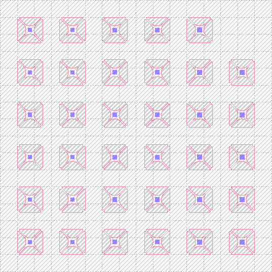
The idea is to obtain a sample with 6x6 trampolines: mechanical structure with a central pad of 100x100 \(\mu\)m suspended above a 300x300 \(\mu\)m basin through 4 narrow tethers of width 15 \(\mu\)m that stick it to the substrate; photonic structure realized as a square array of circular holes with every combination of parameters a [0.9, 1, 1.1] \(\mu\)m (increasing along rows from left to right) and r [145, 150, 165] nm (increasing along columns from bottom to top) repeated in subsets of 4 trampolines.
CAD:
CAD files:
19/06/2026 Sample cleavage + cleaning
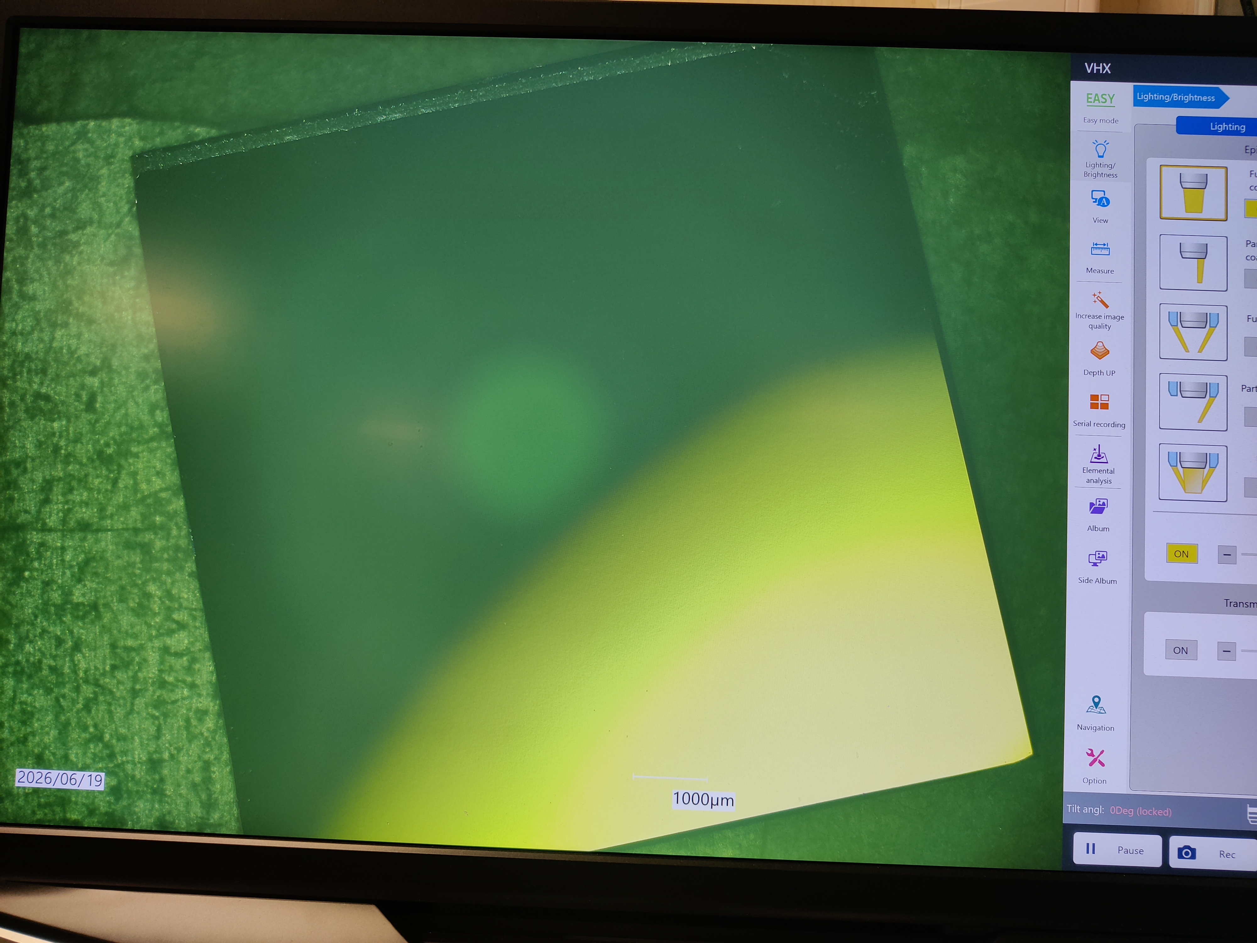
A new chip of 1x1 cm with 300 nm of low-stress SiN was cut. Then it was merged in a becker with ACE and put in a sonicator for about 15 sec, then merged in a becker with IPA and dried with the apposite gun. Looking at the microscope it resulted to be perfectly clean.
Cleaned sample (optical microscope):
23/06/2026 Spin coating, EBL exposure
| Spin&bake | |
|---|---|
| AR.P 6200.13 | 2000 RPM, 1'; 150°C, 1' |
The CAD was built using the gdstk package to create gds files, exploiting the multi-vertex polygons function to draw the circles. Plus, the trampoline in the top-right corner was removed in order to use that vacancy as a marker which corresponds to the corner with parameters (a = 1.1 \(\mu\)m and r = 165 nm) showing the orientation of the chip.
| EBL |
|---|
| EHT: 30 kV |
| Dose: 140 \(\mu\)C/cm\(^2\) |
| step-size: 20 nm |
| filling mode: concentric, outward |
First, we exposed the holes patterns with an aperture of 30 \(\mu\)m (to obtain a current of about 300 pA), using a writefield of 100 \(\mu\)m. Then, we exposed the trampoline masks with an aperture of 60 \(\mu\)m (to obtain a current of about 1 nA) using a writefield of 500 \(\mu\)m.
25/06/2026 Development, RIE etching
| Develop | |
|---|---|
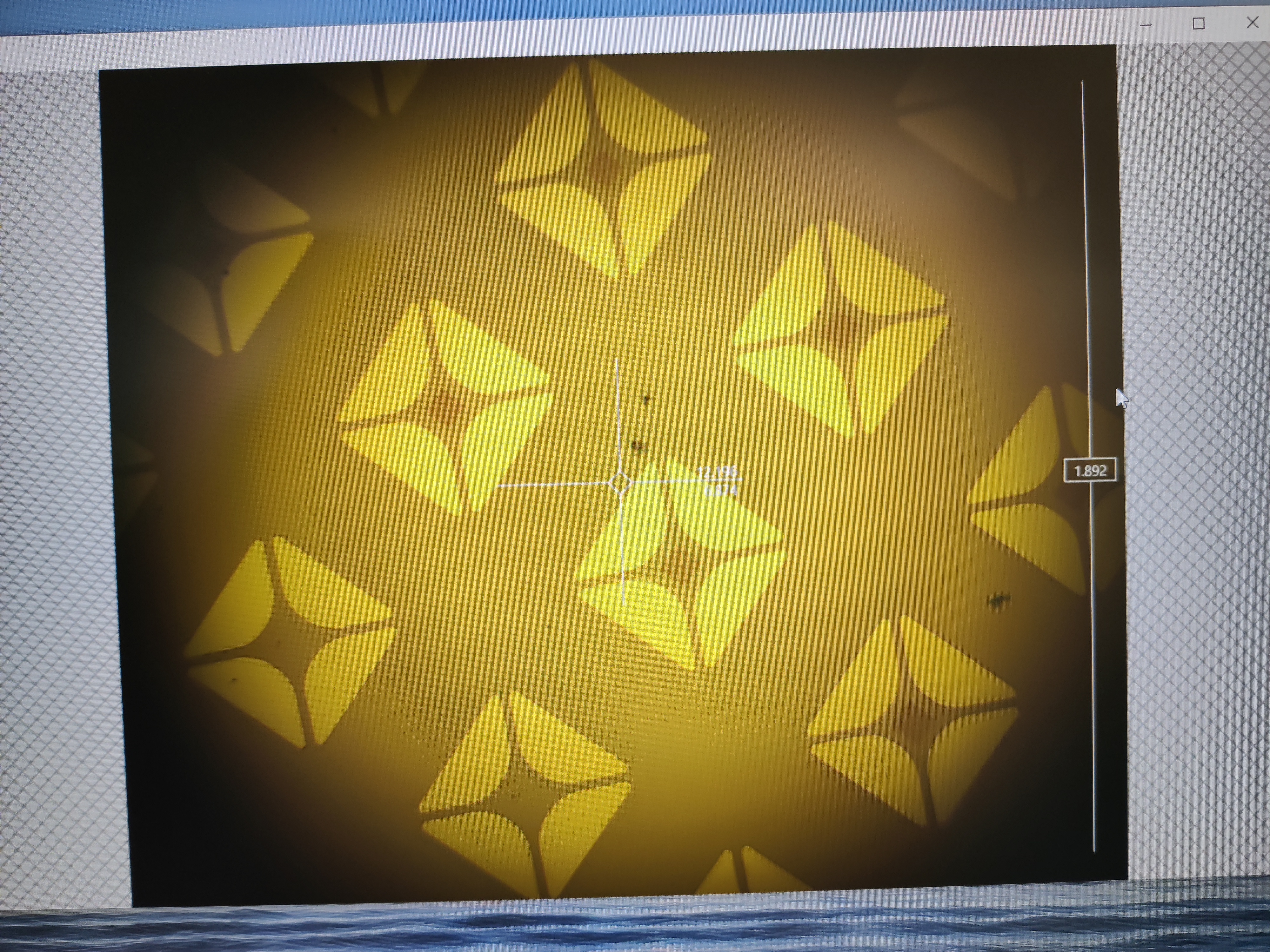
| AR 600-546 | 1' 30'', stop in IPA |
Developed sample (optical microscope):
| RIE |
|---|
| \(SF_6\)/\(O_2\): 32/8 sccm |
| 50 W, time: 5' 30'' |
Then the sample was cleaned to remove all the remaining resist: put the chip in a becker with ACE and turn on the sonicator for 15 sec, then merge it in IPA and dry it. The etching seemed to work well, but unfortunately only the two central rows show the holes pattern on the central plate of the trampolines.
Developed sample (optical microscope):
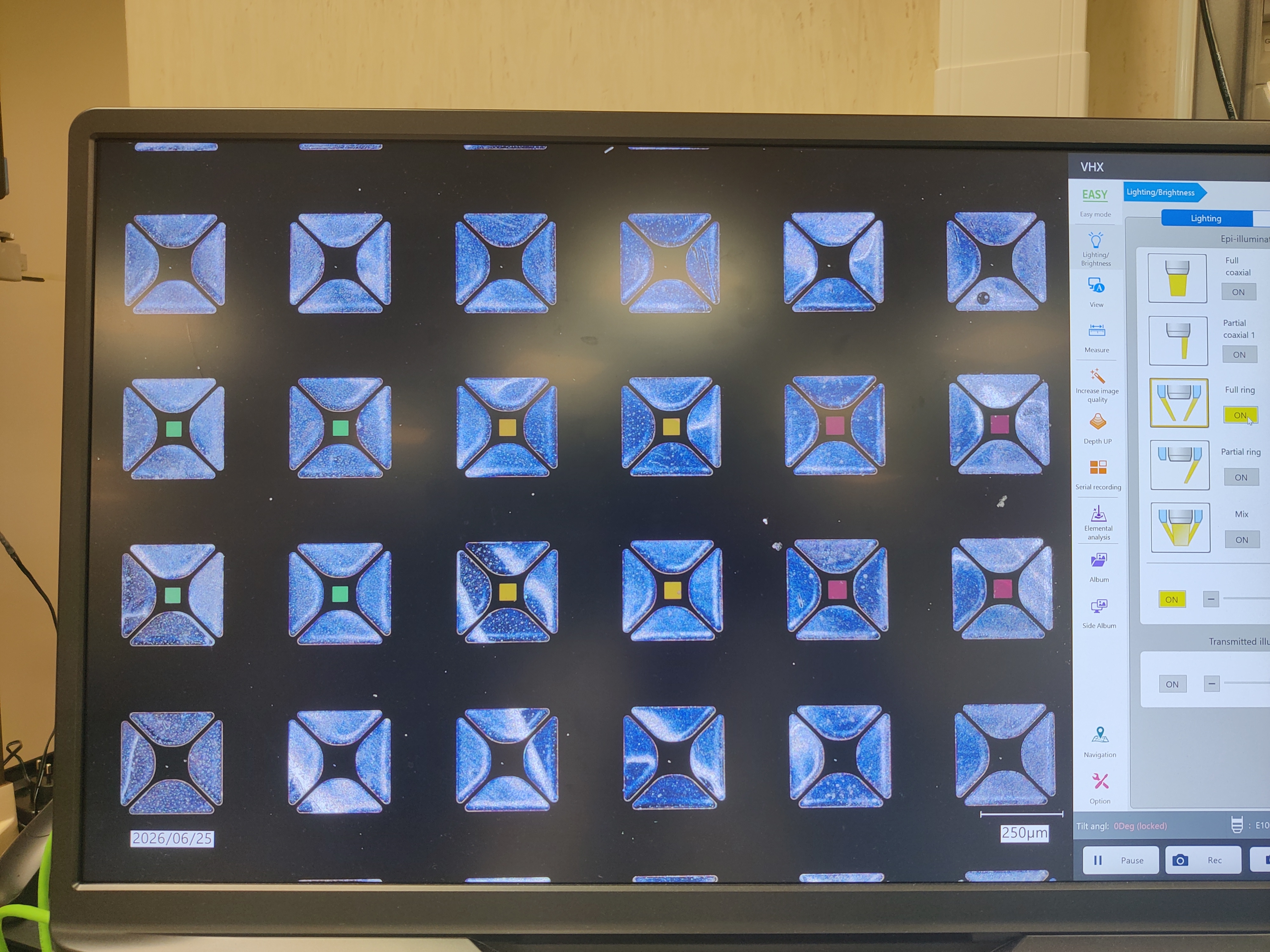
ERROR: some holes pattern present in the CAD were not exposed, this could be due to the anomaly that I noticed during the exposure when the motors led were blocked and the SE2 detector screen was black
26/06/2026 KOH etching
Then the sample was merged into a hot (90°) KOH solution (30%) for 25 min, and finally washed in 3 different becker with DI water and left to dry. Looking at the sample at the optical microscope we noted that there was still some silicon underneath the central pad of the trampolines, so we decided to proceed with a second immersion in KOH.
Etched sample (optical microscope):
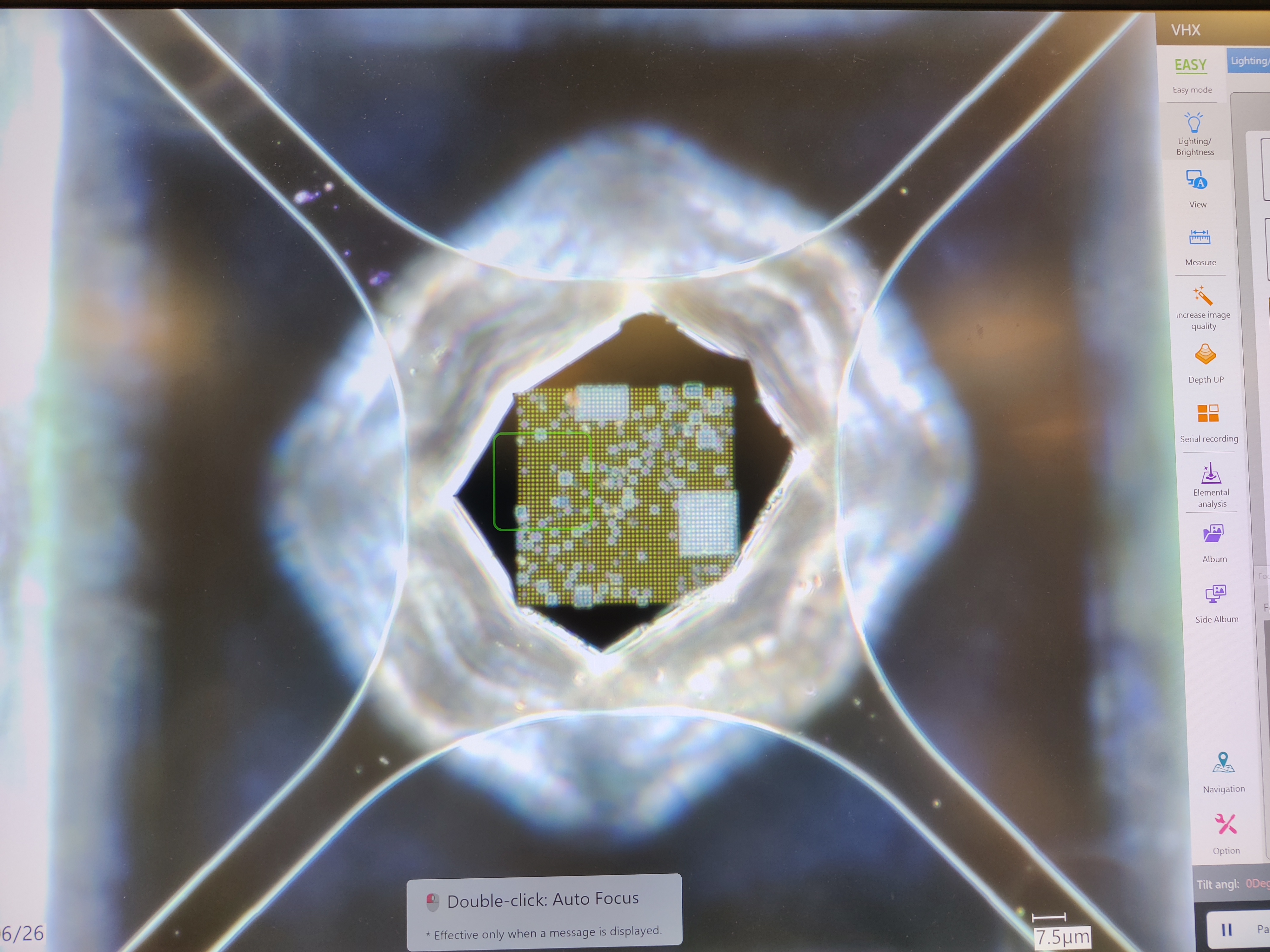
The same KOH process was repeated in the same way merging again the sample for 20 min. In the end, the trampolines were fully suspended and the holes completely opened!.
Etched sample (optical microscope):
