Resis recipes
\(\mathrm{Si_3N_4}\) etching
CSAR AR-P.6200.13
-
AR 300.80
- spin @4000 RPM for 1'
- bake @120/150°C for 1'
-
CSAR AR-P.6200.13
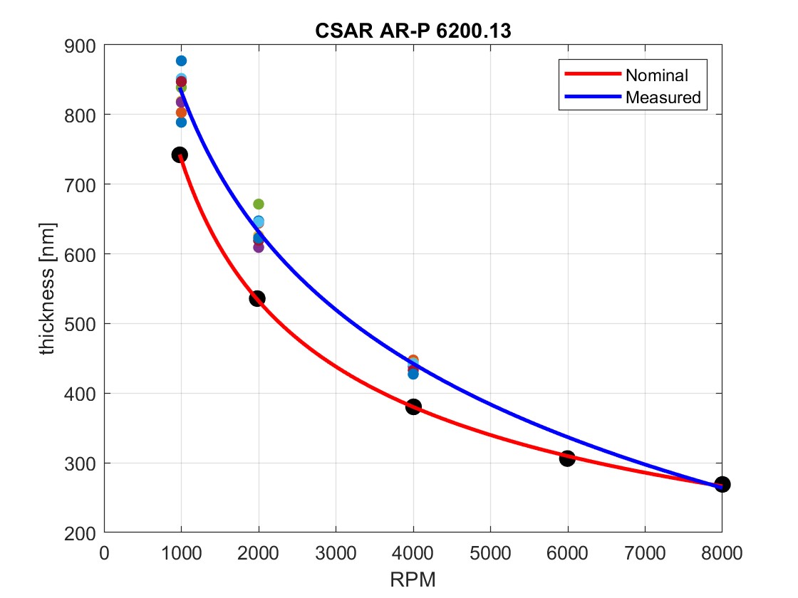
- spin @XXXX RPM (see figure but usually 2000)
- bake @150°C for 1'
-
E-beam average parameters:
- 30 keV, \(140\,\mu\mathrm{C}/\mathrm{cm}^2\), step size: < 60 nm
-
Develop in AR 600.546 for 1' (or 1' 30''?), rinse in IPA, then N₂
-
Etching parameters @RIE Falcon:
- \(\mathrm{SF_6/O_2} = 32/8\ \mathrm{sccm}, P = 6 \times 10^{-2}\ \mathrm{mbar}, 50 \mathrm{W}\)
- 3' etches in excess of 100 nm
CSAR spinning calibration curve:
\(\mathrm{Si_3N_4}\) lift-off
PMMA AR-P 679.04
- spin @4000 RPM for 1'
-
bake @120°C for 15'
-
E-beam average parameters:
- 20 keV, \(240\,\mu\mathrm{C}/\mathrm{cm}^2\), step size: < 40 nm
- Run with aperture \(60\, \mu m\)
-
Develop in AR 600.56 for 1' 30''/2', rinse in IPA, then N₂
-
Lift-off in Hot Acetone @50°C for 15' (or overnight @RT), rinse in IPA then N₂
AR-P 3120
Positive resist, checked for 50nm Au. Before the resist is used an adhesive layer.
-
Ar300-80
- spin @500 RPM for 5'', then @4000 RPM for 1'
- bake @180°C for 2'
-
AR-P 3120
- spin @500 RPM for 5'', then @2000 RPM for 1'
- bake @95°C for 1'
-
Optical lithography parameters @ML3:
- Dose \(350\ \mathrm{mJ/cm^2}\), resolution: \(0.6\ \mathrm{\mu m}\), quality: high
-
Develop in AR 300-26 1:8 for 85", rinse in H₂O for 30"
-
Descum parameters @RIE Falcon:
- 5 W with 30 sccm of O₂
-
Lift-off in Hot Acetone @50°C for 15' (or overnight @RT), rinse in IPA then N₂
LOR 3A and S1805
Two positive resists, checked for 50 nm Au.
The bilayer resist creates an undercut and facilitate lift-off: only S1805 (S1818 is too thick (@2500 RPM for 1' ~2.3 µm) therefore even with 130 dose the LOR under doesn't present undercut) is exposed by UV and dissolved by MF-319 during development. However, since LOR 3A is also soluble in MF-319 (less than LOR 20B), regardless of UV exposure, the developer diffuses laterally beneath S1805 and dissolves the underlying LOR 3A, creating an undercut wider than the lithographic pattern that facilitates lift-off.
- LOR 3A ~350 nm
- prebake @170°C for 5' (hydrophobic, sample must be dried before spin coating but less than LOR 20B because it reacts less to MF-319)
- spin @500 RPM for 5'', then @2500 RPM for 1'
- bake @180°C for 5'
- S1805 ~200 nm
- spin @500 RPM for 5'', then @2500 RPM for 1'
- bake @110°C for 1'
-
Optical lithography parameters @ML3:
- Dose: \(60\ \mathrm{mJ/cm^2}\), quality: high
-
Develop in MF-319 (base) for 75", rinse in H₂O for 30", then N₂
-
Lift-off in Hot Acetone @50°C for 15', or overnight @RT (removes S1818), rinse in IPA, then H₂O, then MF-319 @RT for 10' or @50°C for 5' (removes LOR 3A), rinse in H₂O, then N₂
Si lift-off
PMMA AR-P 679.04
- spin @4000 RPM for 1'
- bake @120°C for 15'
Ga @ NEST (check)
GaAs lift-off
LOR 20B and S1805
Two positive resist, checked for 15/150 nm Cr/Au.
The bilayer resist creates an undercut and facilitates lift-off: only S1805 is exposed by UV and dissolved by MF-319 during development. However, since LOR 20B is also soluble in MF-319, regardless of UV exposure, the developer diffuses laterally beneath S1805 and dissolves the underlying LOR 20B, creating an undercut wider than the lithographic pattern that facilitates lift-off.
- LOR 20B ~1 µm
- prebake @190°C for 5' (hydrophobic, sample must be dried before spin coating)
- spin @500 RPM for 5'', then @2500 RPM for 1'
- bake @190°C for 5'
- S1805 ~200 nm
- spin @500 RPM for 5'', then @2500 RPM for 1'
- bake @110°C for 1'
-
Optical lithography parameters @ML3:
- Dose: \(60\ \mathrm{mJ/cm^2}\), quality: high
-
Develop in MF-319 (base) for 45", rinse in H₂O for 30", then N₂
-
Lift-off in Hot Acetone @50°C for 15', or overnight @RT (removes S1805), rinse in IPA, then H₂O, then MF-319 @RT for 10' or @50°C for 5' (removes LOR 20B), rinse in H₂O, then N₂
S1818
Positive resist, checked for 5nm Ni. Thickness ~1.5 µm. - spin @3000 RPM for 1' - bake @110°C for 1'
-
Optical lithography parameters @ML3:
Dose: \(180\ \mathrm{mJ/cm^2}\), quality: high -
Post-exposure bake @115°C for 20"
-
Develop in MF-319 for 45", rinse in H₂O for 15", then N₂
-
Lift-off in Hot Acetone @50°C for 6' (or overnight @RT), rinse in IPA, then N₂
GaAs etching
AZ-10XT
Used for GaAs active region etching with ICP-RIE. Positive resist, thickness ~1 µm. - spin @3000 RPM for 1' - pake @110°C at 3'
-
Optical lithography parameters @ML3:
- Dose: \(400\ \mathrm{mJ/cm^2}\), quality: normal
-
Develop in AZ 726 MIF (base) for 7', rinse in H₂O, then N₂
-
Removal with AZ 920 @50°C for 10–15' (or overnight @RT), rinse in H₂O, then N₂